



半导体自动化产线 Semiconductor Auto Line
HURAKAN深耕半导体高端智能装备设计领域,聚焦半导体自动化产线设备的专属工业设计与量产落地服务,深谙半导体制造无尘车间、高精度制程、规范化作业的严苛行业标准。团队摒弃纯艺术化的创意表达,完全依托半导体晶圆加工、封装测试、精密分拣等核心生产场景,结合无尘工况、设备联动逻辑、安全生产规范与量产工艺要求,完成从需求拆解、方案迭代、结构合规校核、无尘适配优化、样机调试到批量量产对接的全闭环落地服务。项目全程严控设备装配精度、无尘密封性、结构稳定性与工艺适配性,精准规避高端智能装备常见的设计与量产脱节、场景适配不足、运维难度过高等问题,以严谨的工程思维、丰富的精密设备落地经验,保障每一处设计均可落地、可量产、可运维,充分展现团队硬核、靠谱、务实的高端工业装备设计实操能力。
HURAKAN is deeply engaged in the design field of high-end semiconductor intelligent equipment, focusing on the exclusive industrial design and mass production implementation services of semiconductor automatic production line equipment. We are well versed in the strict industry standards of dust-free workshops, high-precision manufacturing processes and standardized operations in semiconductor manufacturing. Abandoning purely artistic creative expression, we fully rely on the core production scenarios such as semiconductor wafer processing, packaging testing and precision sorting, and complete full closed-loop services from demand decomposition, scheme iteration, structural compliance verification, dust-free adaptation optimization, prototype debugging to batch mass production docking in combination with dust-free working conditions, equipment linkage logic, safety production specifications and mass production process requirements. Throughout the project, we strictly control equipment assembly accuracy, dust-free tightness, structural stability and process adaptability, accurately avoid common problems of high-end intelligent equipment such as disconnection between design and mass production, insufficient scenario adaptation and high operation and maintenance difficulty, and ensure that every design can be implemented, mass-produced and maintained with rigorous engineering thinking and rich experience in precision equipment implementation, fully demonstrating the team’s hard-core, reliable and pragmatic practical capabilities in high-end industrial equipment design.
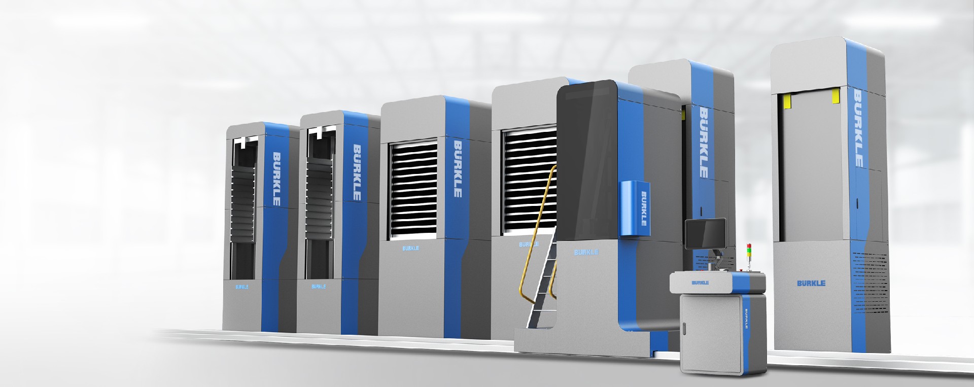
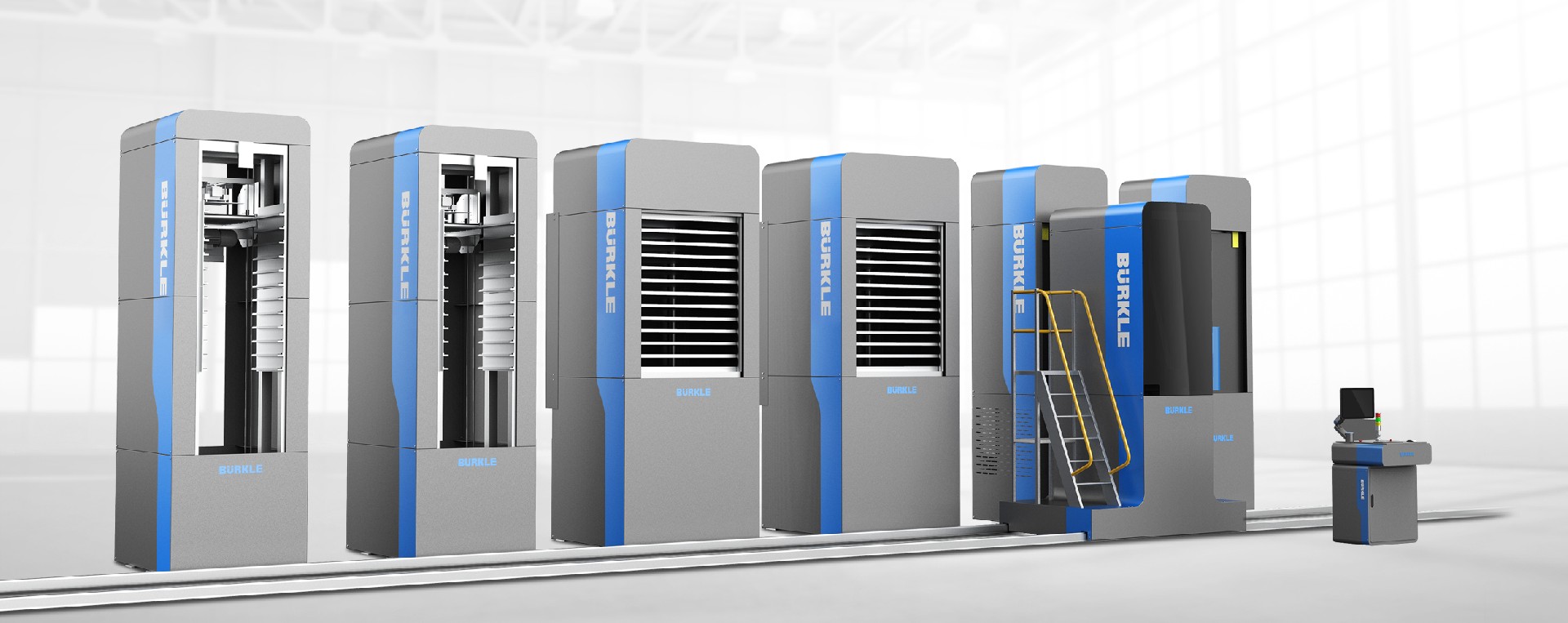
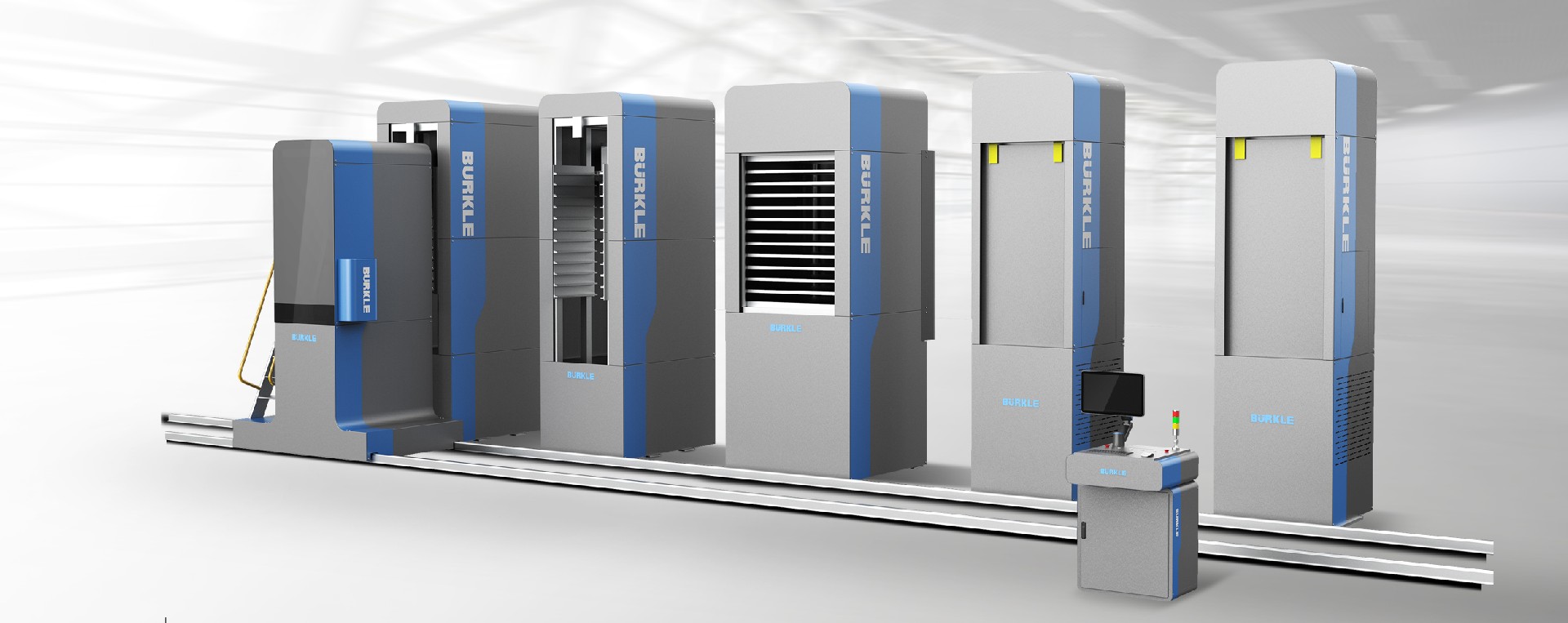
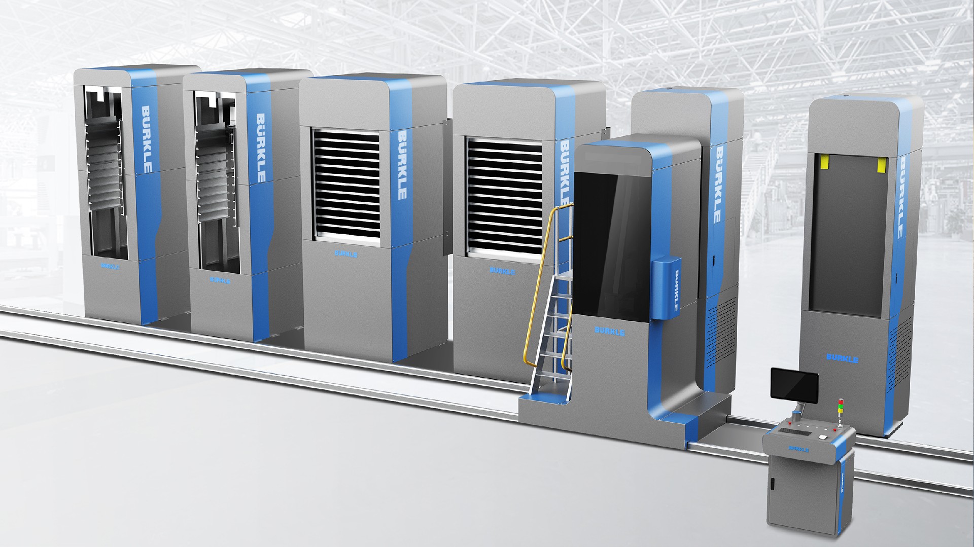
在造型设计层面,团队打破传统半导体产线设备造型笨重、线条杂乱、视觉臃肿、同质化严重的行业弊端,以高端精密装备极简美学为核心,打造适配无尘车间的一体化规整视觉体系。整体采用模块化一体式机身设计,线条平直利落、分区规整有序,弱化大型自动化设备的工业厚重感,契合半导体行业高精尖、洁净、严谨的品牌调性。针对无尘车间洁净、防静电、易清洁的核心需求,甄选防静电无尘烤漆、高致密合金等高端材质,搭配低饱和科技专属配色,有效杜绝粉尘吸附、静电残留、污渍堆积等问题,适配半导体严苛生产环境。同时优化设备整体比例与外饰细节,统一产线设备视觉语言,让单台设备与整线产线高度适配,形成系统化、标准化的高端视觉形象,彻底跳出行业同质化设计内卷,赋予产品极强的高端市场辨识度。
In terms of modeling design, the team breaks the industry drawbacks of traditional semiconductor production line equipment such as bulky shape, messy lines, bloated vision and serious homogenization, and builds an integrated and standardized visual system suitable for dust-free workshops with the minimalism aesthetics of high-end precision equipment as the core. The overall design adopts a modular integrated fuselage with flat and neat lines and regular zoning, weakening the industrial heaviness of large-scale automatic equipment and fitting the high-precision, clean and rigorous brand tone of the semiconductor industry. Aiming at the core requirements of dust-free workshops for cleanliness, anti-static and easy cleaning, we select high-end materials such as anti-static dust-free paint and high-density alloys, matched with exclusive low-saturation technological color schemes, which effectively prevent dust adsorption, static residue and stain accumulation and adapt to the harsh production environment of semiconductors. Meanwhile, we optimize the overall proportion and exterior details of the equipment, unify the visual language of production line equipment, enable single equipment to highly adapt to the whole production line, form a systematic and standardized high-end visual image, completely get rid of the homogeneous design involution in the industry, and endow products with strong high-end market recognition.
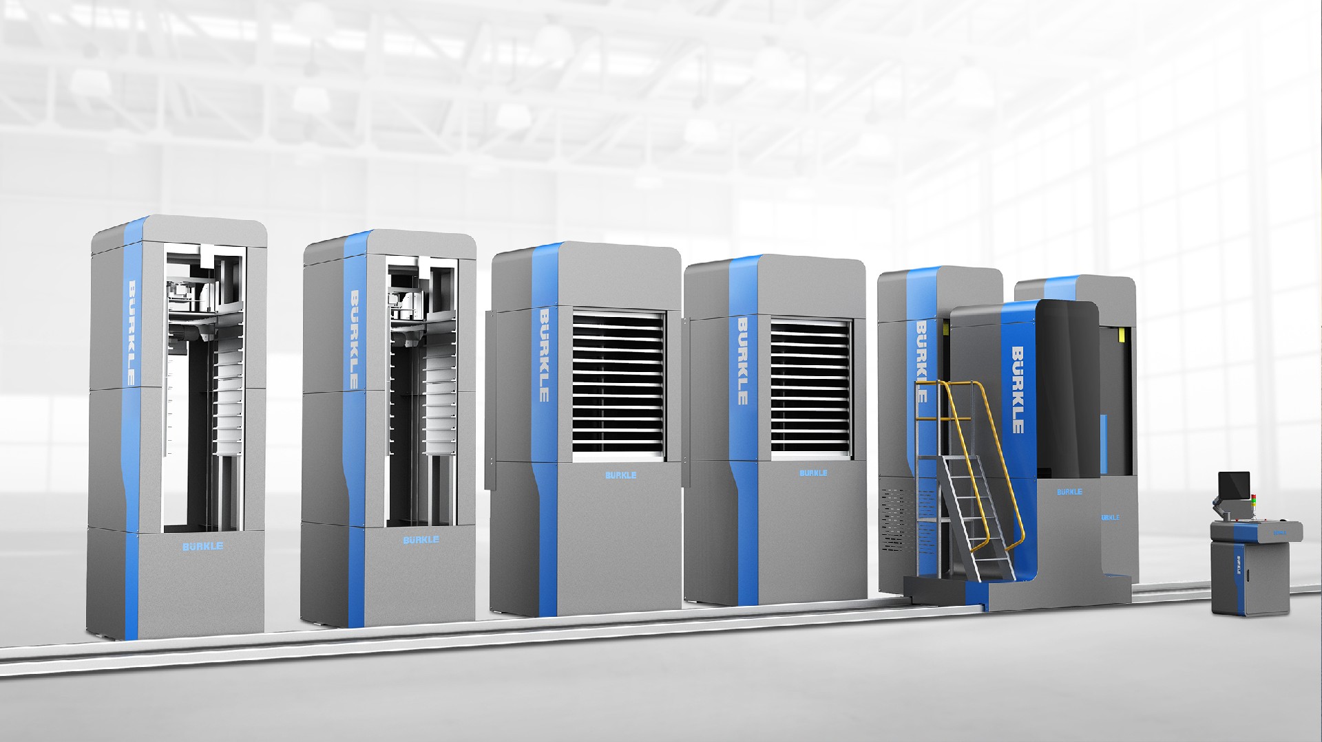
本项目核心创新聚焦精密结构优化与智能化人机交互升级,针对性解决传统半导体产线设备占地冗余、拆装运维繁琐、散热不畅、操作门槛高、人机适配性差等行业痛点。在结构设计上,团队重构设备内部精密模组布局,通过紧凑型集成结构设计,在不影响设备高精度制程性能的前提下,大幅压缩设备占用空间,提升无尘车间场地利用率;优化独立密闭散热与通风除尘结构,兼顾设备持续高负荷运转的散热需求与车间无尘洁净标准,同时采用模块化分体结构,简化设备拆装、检修、零部件更换流程,极大降低后期运维成本与停机损耗。在人机交互层面,贴合产线操作人员常态化作业习惯,重新规划操作屏、物理按键、调试接口的布局位置,升级高清工业触控交互大屏,优化操作视野与人体工学适配角度;简化复杂制程参数调试逻辑,新增制程数据可视化、异常故障智能报警、生产数据溯源、权限分级管理等智能功能,降低专业操作门槛,有效提升产线调试、生产、运维的整体作业效率。
The core innovation of this project focuses on precision structure optimization and intelligent human-computer interaction upgrading, targeting industry pain points of traditional semiconductor production line equipment such as redundant floor space, cumbersome disassembly and maintenance, poor heat dissipation, high operation threshold and poor human-computer adaptability. In terms of structural design, the team reconstructs the internal precision module layout of the equipment, and greatly compresses the equipment occupied space and improves the site utilization rate of dust-free workshops through compact integrated structure design without affecting the high-precision manufacturing performance of the equipment. We optimize the independent closed heat dissipation and ventilation and dust removal structure to meet the heat dissipation requirements of continuous high-load operation of the equipment and the dust-free cleanliness standards of the workshop. At the same time, the modular split structure is adopted to simplify the disassembly, inspection and parts replacement process of the equipment, greatly reducing the later operation and maintenance costs and shutdown losses. At the human-computer interaction level, we conform to the daily operation habits of production line operators, redesign the layout of operation screens, physical buttons and debugging interfaces, upgrade the high-definition industrial touch interactive large screen, and optimize the operation vision and ergonomic adaptation angle. We simplify the debugging logic of complex process parameters, and add intelligent functions such as visualized process data, intelligent abnormal fault alarm, production data traceability and hierarchical authority management, lowering the professional operation threshold and effectively improving the overall operation efficiency of production line debugging, production and operation maintenance.
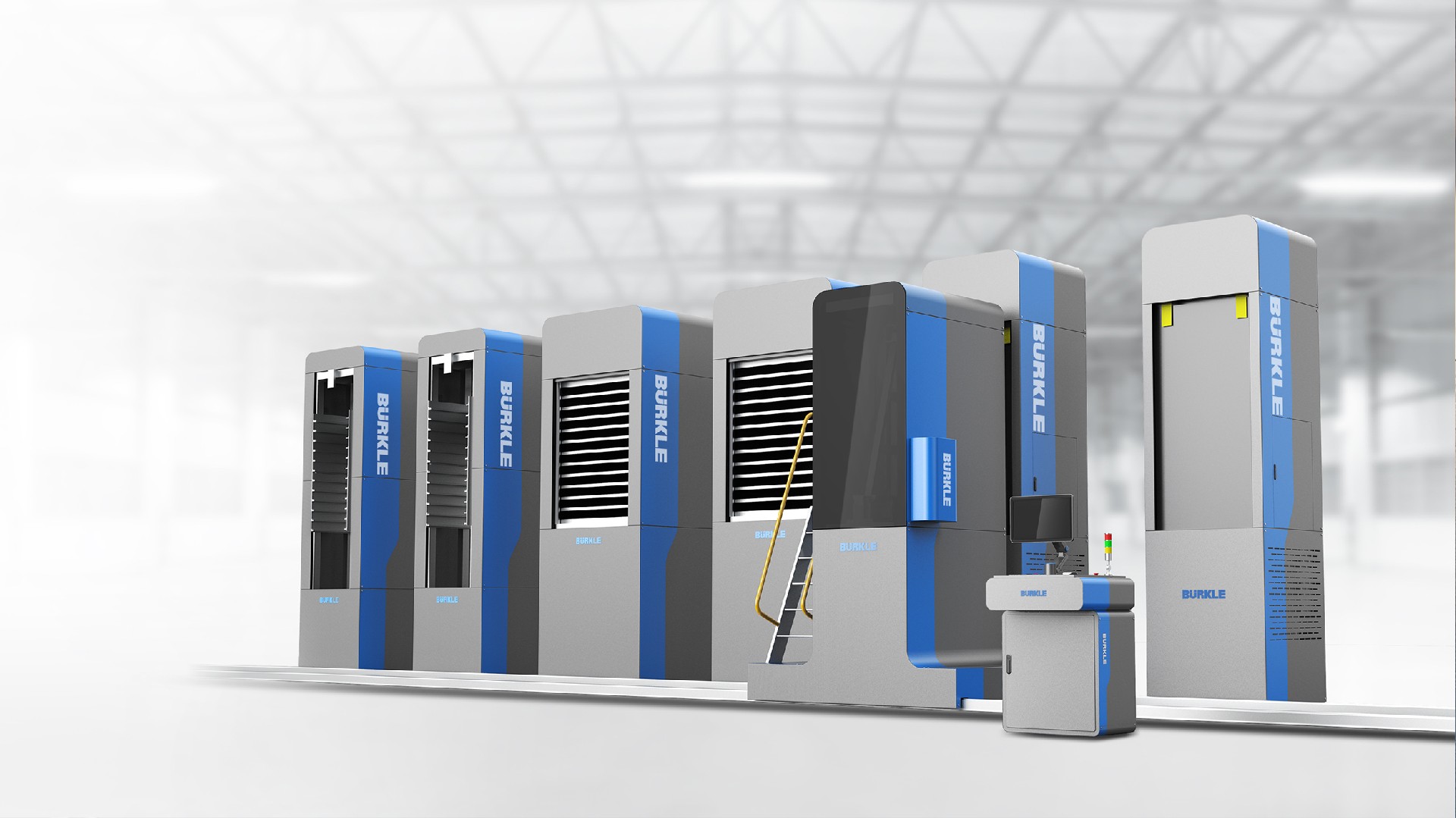
凭借系统化的创新设计与成熟的量产落地能力,本次半导体自动化产线设备为客户创造了显著的商业增量价值,助力客户抢占高端半导体智能装备细分市场。设备高端规整的外观质感、标准化的模块化设计与洁净适配的工艺体系,彻底改变客户原有产品低端、老旧的市场形象,成功助力客户切入头部半导体企业、晶圆制造工厂、高端封装测试企业的供应链体系,实现大幅产品溢价,与行业中低端同质化竞品构建清晰的市场竞争壁垒。优化后的紧凑结构、稳定的制程性能、便捷的人机运维体验,大幅提升终端客户使用满意度与合作粘性,有效提升产品复购率与行业口碑。同时标准化量产结构有效降低客户生产开模、装配调试、售后运维的综合成本,提升批量交付效率。产品落地量产投放市场后,客户产线设备订单量持续增长,市场占有率稳步提升,核心竞争力全面升级,稳固了其在半导体自动化装备领域的高端市场地位。
With systematic innovative design and mature mass production implementation capabilities, this semiconductor automatic production line equipment has created significant incremental commercial value for clients and helped them seize the segmented market of high-end semiconductor intelligent equipment. The high-end and regular appearance texture, standardized modular design and process system adapted to cleanliness completely change the low-end and outdated market image of the client’s original products, successfully help the client enter the supply chain system of leading semiconductor enterprises, wafer manufacturing factories and high-end packaging and testing enterprises, achieve substantial product premium, and build clear market competition barriers with low and medium-end homogeneous competing products in the industry. The optimized compact structure, stable process performance and convenient human-computer operation and maintenance experience greatly improve the end-user satisfaction and cooperation stickiness, and effectively increase the product repurchase rate and industry reputation. Meanwhile, the standardized mass production structure effectively reduces the client’s comprehensive costs of production mold opening, assembly debugging and after-sales operation and maintenance, and improves the batch delivery efficiency. After the product is mass-produced and launched into the market, the client’s production line equipment orders continue to grow, the market share increases steadily, the core competitiveness is fully upgraded, and its high-end market position in the field of semiconductor automatic equipment is consolidated.
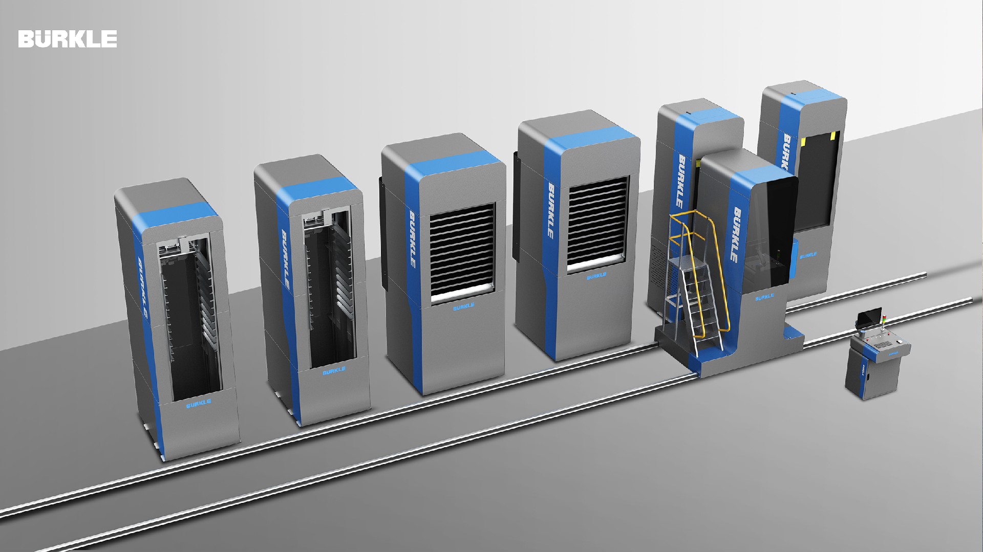
HURAKAN始终坚守“设计落地赋能高端装备产业升级”的核心服务理念,深耕半导体、精密智能装备等高端制造领域,坚持拒绝脱离工况标准、量产工艺与商业逻辑的概念化设计。本次半导体自动化产线项目,以半导体严苛生产场景为基石,以造型设计重塑高端装备视觉标准,以结构创新保障设备制程稳定性,以人机优化降低生产运维成本,通过全链路、高精密、可落地的工业设计服务,实现产品颜值、性能、体验与商业价值的多维升级。未来,HURAKAN将持续聚焦高端精密工业装备赛道,以严谨的工程落地经验与前沿的创新设计思维,持续为高端制造客户打造高精密、高适配、高溢价、高竞争力的标杆级产品,持续助力品牌深耕高端细分市场,领跑智能制造产业升级浪潮。
HURAKAN always adheres to the core service philosophy of "design implementation empowers the upgrading of high-end equipment industry", deeply engages in high-end manufacturing fields such as semiconductors and precision intelligent equipment, and insists on rejecting conceptual design divorced from working condition standards, mass production processes and commercial logic. Based on the harsh production scenarios of semiconductors, this semiconductor automatic production line project reshapes the visual standards of high-end equipment through modeling design, guarantees the stability of equipment manufacturing processes through structural innovation, and reduces production and operation maintenance costs through human-computer optimization. It realizes the multi-dimensional upgrading of product appearance, performance, experience and commercial value through full-link, high-precision and implementable industrial design services. In the future, HURAKAN will continue to focus on the track of high-end precision industrial equipment, and continuously create benchmark products with high precision, high adaptation, high premium and high competitiveness for high-end manufacturing clients with rigorous engineering implementation experience and cutting-edge innovative design thinking, helping brands deepen high-end segmented markets and lead the intelligent manufacturing industry upgrading trend.



Microblog