

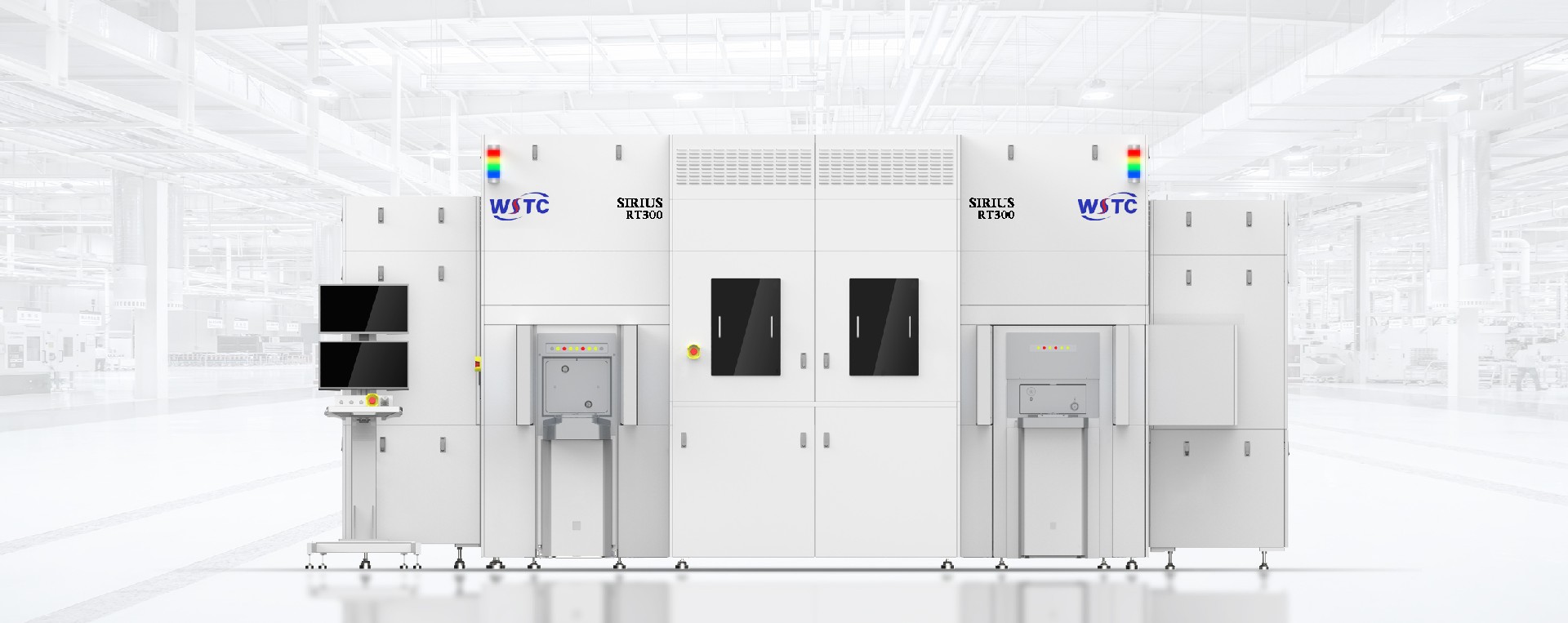


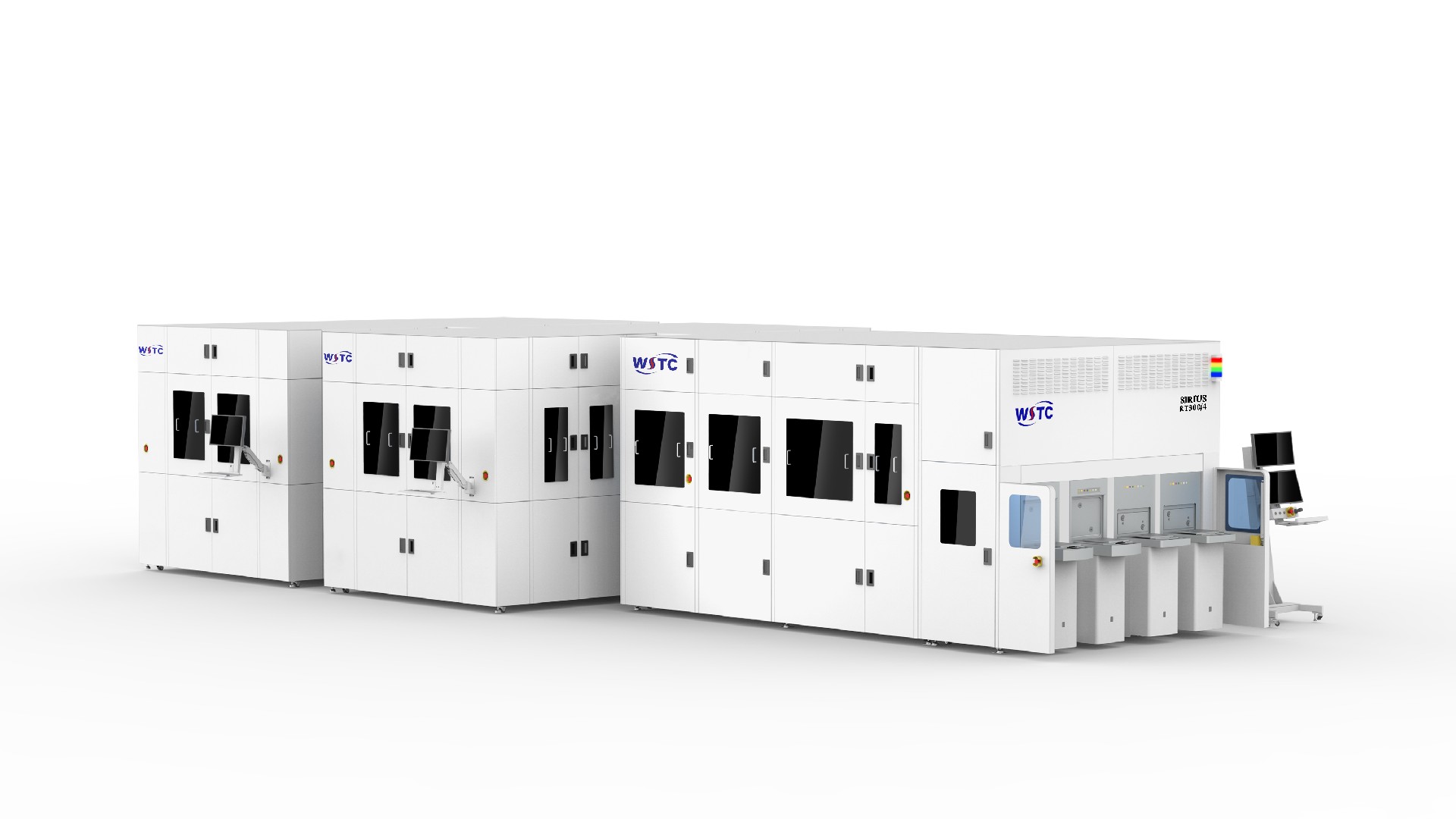
半导体混合键合机 Hybrid Bonding Equipment
HURAKAN全程主导半导体混合键合机工业设计全链路落地工作,深耕半导体先进封装高端精密装备领域,严格遵循无尘车间制程规范、半导体精密设备安全标准与量产工艺体系,完成市场调研、方案迭代、结构合规校核、工况人机适配、样机调试到批量量产落地跟进的全流程实操服务。团队深度结合混合键合设备微纳级精密对位、低温键合、无尘封装、长时间连续作业的核心特性,摒弃理想化概念设计,针对性解决设备微震抑制、腔体洁净密封、精密模组防护、运维工艺适配等落地难题,以扎实的高端半导体装备工程经验,为客户交付高精密、高稳定、可量产的一体化工业设计解决方案。
HURAKAN fully leads the full-link industrial design and mass production implementation of the semiconductor hybrid bonding machine. Focusing on the field of high-end precision equipment for advanced semiconductor packaging, we strictly comply with dust-free workshop process specifications, semiconductor precision equipment safety standards and mass production process systems, completing full-process practical services from market research, scheme iteration and structural compliance verification to working condition human-computer adaptation, prototype debugging and batch production follow-up. Combined with the core characteristics of micro-nano level precision alignment, low-temperature bonding, dust-free packaging and long-term continuous operation of hybrid bonding equipment, we abandon idealized conceptual design and solve key landing problems such as equipment micro-vibration suppression, cavity clean sealing, precision module protection and operation and maintenance process adaptation. With solid engineering experience in high-end semiconductor equipment, we deliver high-precision, stable and mass-producible integrated industrial design solutions for clients.
本次项目在造型美学、精密结构、工业人机交互三大维度完成全方位创新升级,有效解决传统混合键合设备外观呆板粗犷、整机集成度低、精密防护不足、调试操作繁琐、工况适配性弱的行业痛点。造型采用一体化全封闭极简机身设计,线条平整克制、结构层次规整,摒弃传统工业设备的厚重廉价质感,塑造精密洁净、严谨高端的先进半导体装备视觉形态,适配晶圆封装车间、芯片研发实验室、先进制程产业园等高端场景;结构上重构整机内部模组布局、减震防抖架构与无尘密封腔体,优化精密传动防护、恒温控温结构,从物理层面提升键合对位精度与制程稳定性,杜绝粉尘、震动、温差对微纳封装工艺的干扰;人机交互层面贴合精密量产与实验调试双重作业逻辑,简化操作层级与参数调节流程,实现设备操控轻量化、状态可视化、运维智能化的全面升级。
This project achieves all-round innovative upgrades in styling aesthetics, precision structure and industrial human-computer interaction, effectively solving the industry pain points of traditional hybrid bonding equipment such as rigid and rough appearance, low overall integration, insufficient precision protection, cumbersome debugging operation and weak working condition adaptability. The integrated fully enclosed minimalist fuselage with flat and restrained lines and regular structural layers abandons the heavy and cheap texture of traditional industrial equipment, creating a precise, clean, rigorous and high-end visual form of advanced semiconductor equipment, suitable for high-end scenarios such as wafer packaging workshops, chip R&D laboratories and advanced process industrial parks. We reconstruct the internal module layout, shock absorption and anti-vibration architecture and dust-free sealed cavity, optimize precision transmission protection and constant temperature control structure, improve bonding alignment accuracy and process stability at the physical level, and eliminate the interference of dust, vibration and temperature difference on micro-nano packaging processes. In terms of human-computer interaction, we conform to the dual operation logic of precision mass production and experimental debugging, simplify operation levels and parameter adjustment processes, and realize comprehensive upgrading of lightweight equipment control, visualized status and intelligent operation and maintenance.
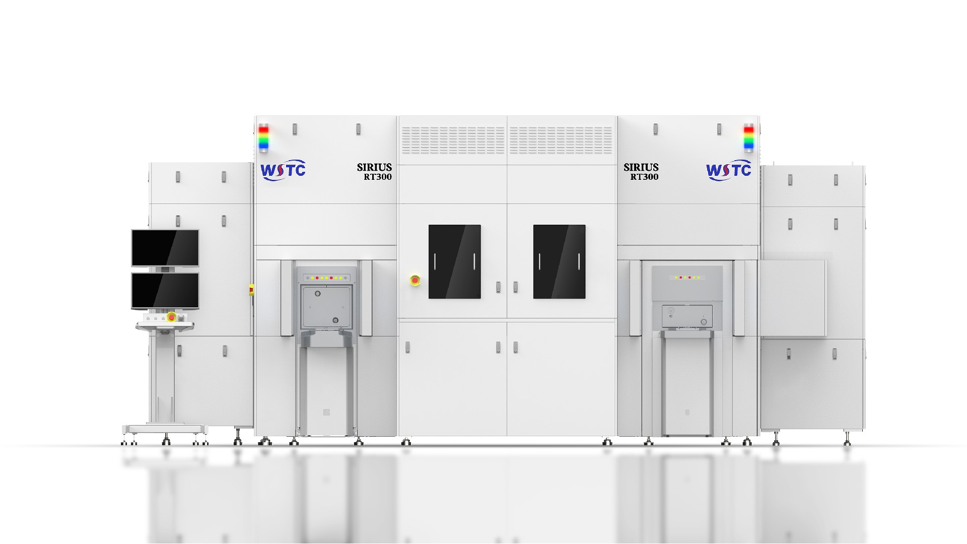
HURAKAN针对半导体无尘精密制程场景精细化打磨产品视觉体系,采用高端精密装备专属低饱和工业配色与模块化极简设计语言,搭配无尘抗污、易清洁、高刚性的钣金工艺,打造洁净统一、秩序规整、辨识度极高的专业设备形态。区别于市面同类封装设备结构外露、造型杂乱、质感廉价、同质化严重的弊端,本次设计紧扣半导体先进封装行业精密、洁净、高端的核心调性,构建专属品牌视觉识别体系,既满足无尘车间严苛的环境使用标准,又依靠差异化外观跳出市场同质化竞争,显著提升产品高端装备质感与场景适配能力,强化品牌在先进封装设备赛道的视觉竞争力。
HURAKAN refines the product visual system for semiconductor dust-free precision process scenarios. Adopting exclusive low-saturation industrial color matching for high-end precision equipment, minimalist modular design language and dust-proof, anti-fouling, easy-to-clean and high-rigidity sheet metal technology, it creates a professional equipment form with clean unity, regular order and high recognition. Different from similar packaging equipment on the market with exposed structures, messy shapes, cheap texture and serious homogenization, this design closely follows the core tone of precision, cleanliness and high-end in the advanced semiconductor packaging industry and builds an exclusive brand visual system. It not only meets the strict environmental standards of dust-free workshops, but also gets rid of market homogenization competition with differentiated appearance, significantly improving the product's high-end equipment texture and scenario adaptation capability, and strengthening the brand's visual competitiveness in the advanced packaging equipment track.
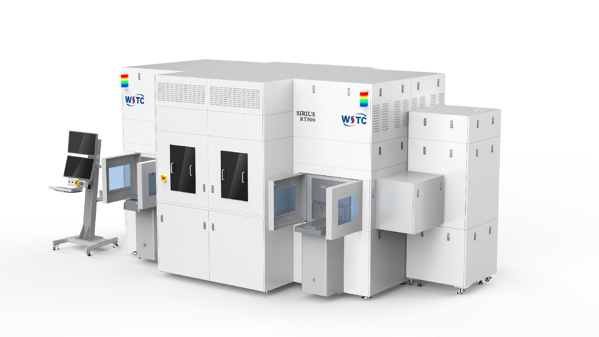
团队从精密制程保障、无尘工况运维、量产标准化降本维度完成深度优化,结合微纳键合高精度作业需求与车间标准化流程,科学规划触控交互区、制程观测窗、精密检修口与线路收纳区域,精简设备启停、参数校准、制程监测、故障复位等核心操作,大幅降低人工干预误差,有效提升芯片封装良率与生产效率。同时全方位优化整机密闭防尘、减震稳频、恒温防护结构,从结构源头规避制程污染、微震偏移、温度波动等工艺风险,保障设备长时间连续精密运行的稳定性。通过统一模块化装配标准、精简冗余结构,有效降低量产装配难度、生产损耗与后期运维故障率,大幅提升设备量产落地性与工程实用性。
The team conducts in-depth optimization from the dimensions of precision process guarantee, dust-free working condition operation and maintenance, and standardized mass production cost reduction. According to the high-precision operation requirements of micro-nano bonding and standardized workshop processes, we scientifically plan the touch interaction area, process observation window, precision maintenance port and circuit storage area, streamline core operations such as equipment start-stop, parameter calibration, process monitoring and fault reset, greatly reducing manual intervention errors and effectively improving chip packaging yield and production efficiency. Meanwhile, we fully optimize the fully enclosed dust-proof, vibration frequency stabilization and constant temperature protection structures to avoid process risks such as process pollution, micro-vibration deviation and temperature fluctuation from the structural source, ensuring the stability of long-term continuous precision operation. By unifying modular assembly standards and streamlining redundant structures, we effectively reduce mass production difficulty, production losses and later maintenance failure rates, and greatly improve the mass production feasibility and engineering practicability of the equipment.
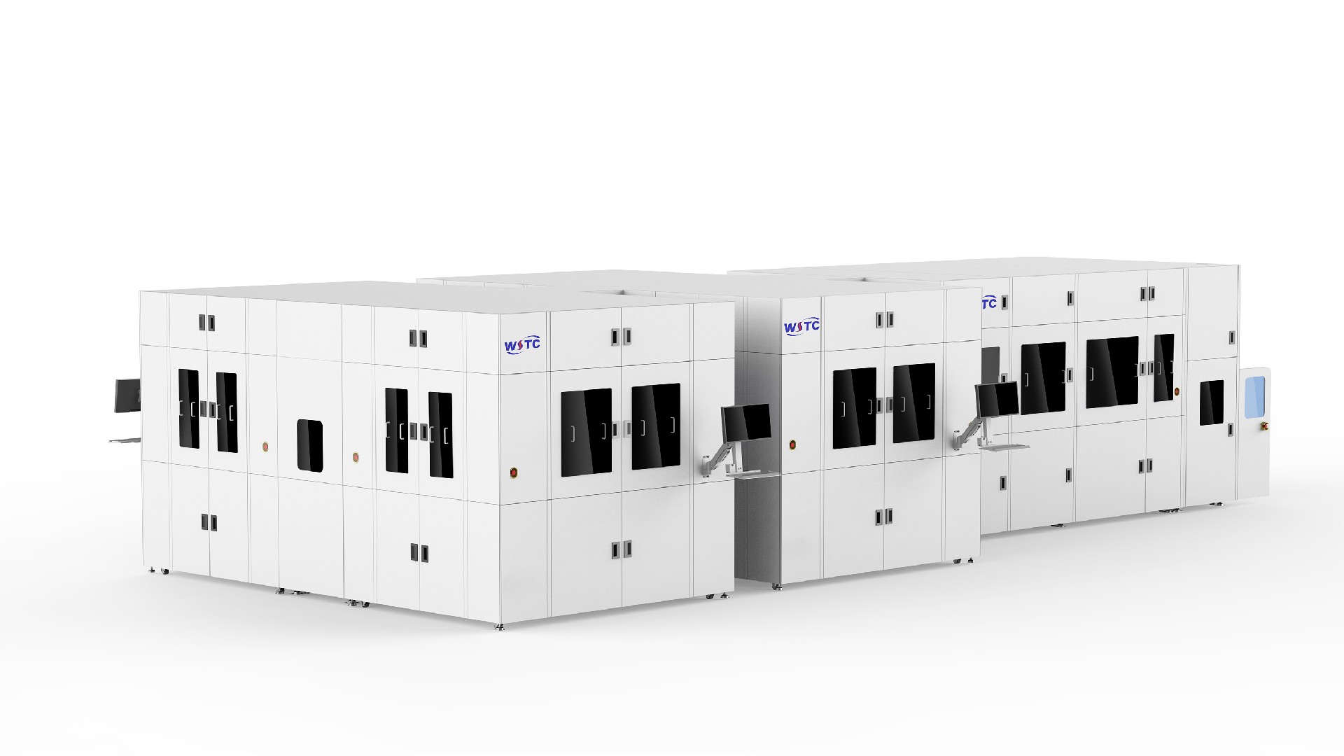
整套设计方案成功落地量产后,该款半导体混合键合机凭借精密高端的外观质感、稳定可靠的微纳制程性能、低耗高效的运维优势,助力客户完成产品迭代升级与品牌高端化重塑。产品顺利切入中高端先进封装装备市场,彻底摆脱行业低端同质化价格内卷,形成强劲的产品溢价与技术竞争壁垒;凭借优异的制程适配性与稳定的加工精度,产品广泛覆盖三维堆叠封装、异构集成、晶圆级封装等高端半导体核心领域,项目中标率与批量订单持续攀升,全方位夯实客户在先进精密封装装备赛道的龙头地位,持续为品牌创造长期稳定的规模化商业价值与权威的行业口碑。
After the successful mass production of the complete design solution, the semiconductor hybrid bonding machine helps clients complete product iteration and high-end brand remodeling with its precise and high-end appearance, stable and reliable micro-nano process performance and low-consumption and high-efficiency operation and maintenance advantages. The product successfully enters the mid-to-high-end advanced packaging equipment market, completely gets rid of low-end industrial homogenization price involution, and forms strong product premium and technical competition barriers. With excellent process adaptability and stable processing accuracy, it widely covers high-end core semiconductor fields such as 3D stack packaging, heterogeneous integration and wafer-level packaging, with continuous growth in project winning rates and bulk orders. It comprehensively consolidates the client's leading position in the advanced precision packaging equipment track, and continuously creates long-term, stable and large-scale commercial value and authoritative industry reputation for the brand.



Microblog